- 您现在的位置:买卖IC网 > Sheet目录2000 > IDTCV119EPVG8 (IDT, Integrated Device Technology Inc)IC CLK GEN DESKTOP PC 48-SSOP
COMMERCIALTEMPERATURERANGE
IDTCV119E
CLOCKGENERATORFORDESKTOPPCPLATFORMS
1
JANUARY 2004
IDTCV119E
COMMERCIAL TEMPERATURE RANGE
CLOCK GENERATOR FOR
DESKTOP PC PLATFORMS
XTAL
Osc Amp
SM Bus
Controller
Watch Dog
Timer
Control
Logic
CPU CLK
Output Buffers
3V66/PCI
Output Buffers
SRC CLK
Output Buffer
48MHz
Output Buffer
X1
X2
SDATA
SCLK
VTT_PWRGD
FS[1:0]
SEL24_48#
IREF
CPU[1:0]
CPU_ITP
REF 1.0
PCI[5:0], PCIF[2:0]
3V66[3:1]
SRC
48MHz[1:0]
PLL3
SSC
PLL4
PLL1
SSC
EasyN
Programming
PLL2
SSC
EasyN
Programming
RESET#
The IDT logo is a registered trademark of Integrated Device Technology, Inc.
2004 Integrated Device Technology, Inc.
DSC-6551/7
FEATURES:
4 PLL architecture
Linear frequency programming
Independent frequency programming and SSC control
Band-gap circuit for differential output
High power-noise rejection ratio
66MHz to 533MHz CPU frequency
VCO frequency up to 1.1G
Support index block read/write, single cycle index block read
Programmable REF, 3V66, PCI, 48MHz I/O drive strength
Programmable 3V66 and PCI Skew
Available in SSOP package
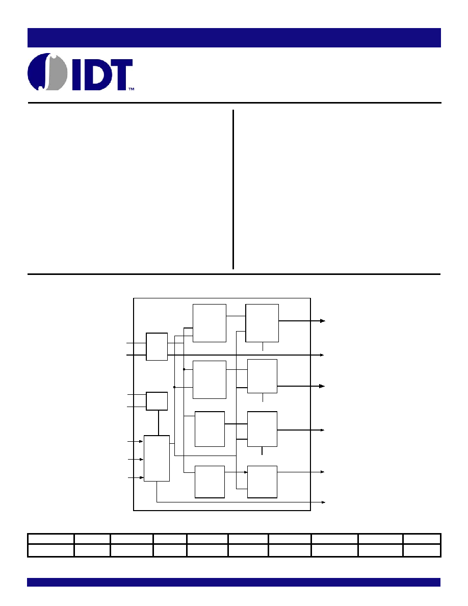
FUNCTIONAL BLOCK DIAGRAM
DESCRIPTION:
IDTCV119E is a 48 pin clock generation device for desktop PC platforms.
ThischipincorporatesfourPLLstoallowindependentgenerationofCPU,AGP/
PCI, SRC, and 48MHz clocks. The dedicated PLL for Serial ATA clock
provides high accuracy frequency. This device also implements Band-gap
referenced IREF to reduce the impact of VDD variation on differential outputs,
which can provide more robust system performance.
Static PLL frequency divide error can be as low as 36 ppm, providing high
accuracy output clock. Each CPU, AGP/PCI, SRC clock has its own Spread
Spectrumselection.
KEY SPECIFICATION:
CPU/SRC CLK cycle to cycle jitter < 125ps
SATA CLK cycle to cycle jitter < 125ps
PCI CLK cycle to cycle jitter < 250ps
Static PLL frequency divide error as low as 36 ppm
OUTPUTTABLE
CPU (Pair)
3V66
3V66/VCH
PCI
PCIF
REF
48MHz
24 - 48MHz
SRC (Pair)
Reset#
33
1
6
322
0
1
发布紧急采购,3分钟左右您将得到回复。
相关PDF资料
IDTCV133PAG
IC FLEXPC CLK PROGR P4 56-TSSOP
IDTCV136PAG
IC FLEXPC CLK ATI RS400 56-TSSOP
IDTCV137PAG
IC FLEXPC CLK AMD K8 56-TSSOP
IDTCV142PAG
IC FLEXPC CLK PROGR P4 56-TSSOP
IDTCV146PVG
IC FLEXPC CLK PROGR P4 56-SSOP
IDTCV149PAG
IC FLEXPC CLK PROGR K8 56-TSSOP
IDTNW6005ASG
IC CALLER ID DECODER 20SOIC
IDTNW6006AS
IC CALLER ID DECODER 20-SOIC
相关代理商/技术参数
IDTCV122C
制造商:IDT 制造商全称:Integrated Device Technology 功能描述:PROGRAMMABLE FLEXPC? CLOCK FOR P4 PROCESSOR
IDTCV122CPVG
功能描述:IC FLEXPC CLK PROGR P4 56-SSOP RoHS:是 类别:集成电路 (IC) >> 时钟/计时 - 专用 系列:FlexPC™ 标准包装:28 系列:- 类型:时钟/频率发生器 PLL:是 主要目的:Intel CPU 服务器 输入:时钟 输出:LVCMOS 电路数:1 比率 - 输入:输出:3:22 差分 - 输入:输出:无/是 频率 - 最大:400MHz 电源电压:3.135 V ~ 3.465 V 工作温度:0°C ~ 85°C 安装类型:表面贴装 封装/外壳:64-TFSOP (0.240",6.10mm 宽) 供应商设备封装:64-TSSOP 包装:管件
IDTCV122CPVG8
功能描述:IC FLEXPC CLK PROGR P4 56-SSOP RoHS:是 类别:集成电路 (IC) >> 时钟/计时 - 专用 系列:FlexPC™ 标准包装:28 系列:- 类型:时钟/频率发生器 PLL:是 主要目的:Intel CPU 服务器 输入:时钟 输出:LVCMOS 电路数:1 比率 - 输入:输出:3:22 差分 - 输入:输出:无/是 频率 - 最大:400MHz 电源电压:3.135 V ~ 3.465 V 工作温度:0°C ~ 85°C 安装类型:表面贴装 封装/外壳:64-TFSOP (0.240",6.10mm 宽) 供应商设备封装:64-TSSOP 包装:管件
IDTCV123
制造商:IDT 制造商全称:Integrated Device Technology 功能描述:PROGRAMMABLE FLEXPC CLOCK FOR P4 PROCESSOR
IDTCV123PV
功能描述:IC FLEXPC CLK PROGR P4 56-SSOP RoHS:否 类别:集成电路 (IC) >> 时钟/计时 - 专用 系列:FlexPC™ 标准包装:1,500 系列:- 类型:时钟缓冲器/驱动器 PLL:是 主要目的:- 输入:- 输出:- 电路数:- 比率 - 输入:输出:- 差分 - 输入:输出:- 频率 - 最大:- 电源电压:3.3V 工作温度:0°C ~ 70°C 安装类型:表面贴装 封装/外壳:28-SSOP(0.209",5.30mm 宽) 供应商设备封装:28-SSOP 包装:带卷 (TR) 其它名称:93786AFT
IDTCV123PV8
功能描述:IC FLEXPC CLK PROGR P4 56-SSOP RoHS:否 类别:集成电路 (IC) >> 时钟/计时 - 专用 系列:FlexPC™ 标准包装:1,500 系列:- 类型:时钟缓冲器/驱动器 PLL:是 主要目的:- 输入:- 输出:- 电路数:- 比率 - 输入:输出:- 差分 - 输入:输出:- 频率 - 最大:- 电源电压:3.3V 工作温度:0°C ~ 70°C 安装类型:表面贴装 封装/外壳:28-SSOP(0.209",5.30mm 宽) 供应商设备封装:28-SSOP 包装:带卷 (TR) 其它名称:93786AFT
IDTCV123PVG
功能描述:IC FLEXPC CLK PROGR P4 56-SSOP RoHS:是 类别:集成电路 (IC) >> 时钟/计时 - 专用 系列:FlexPC™ 标准包装:1,500 系列:- 类型:时钟缓冲器/驱动器 PLL:是 主要目的:- 输入:- 输出:- 电路数:- 比率 - 输入:输出:- 差分 - 输入:输出:- 频率 - 最大:- 电源电压:3.3V 工作温度:0°C ~ 70°C 安装类型:表面贴装 封装/外壳:28-SSOP(0.209",5.30mm 宽) 供应商设备封装:28-SSOP 包装:带卷 (TR) 其它名称:93786AFT
IDTCV123PVG8
功能描述:IC FLEXPC CLK PROGR P4 56-SSOP RoHS:是 类别:集成电路 (IC) >> 时钟/计时 - 专用 系列:FlexPC™ 标准包装:28 系列:- 类型:时钟/频率发生器 PLL:是 主要目的:Intel CPU 服务器 输入:时钟 输出:LVCMOS 电路数:1 比率 - 输入:输出:3:22 差分 - 输入:输出:无/是 频率 - 最大:400MHz 电源电压:3.135 V ~ 3.465 V 工作温度:0°C ~ 85°C 安装类型:表面贴装 封装/外壳:64-TFSOP (0.240",6.10mm 宽) 供应商设备封装:64-TSSOP 包装:管件